
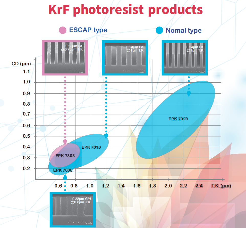
Ⅰ、EPK 7008 Series
Resist Film Thickness:0.8~2.6um
Property:
1. High resolution @0.2um;
2. Excellent etching resistance;
3. High thermal resistance.
Ⅱ、Application Fields
1.Logic Chips:
Applied to lithography for key layers such as Poly, Active Area (AA), Contact and Metal at technology nodes from 90 nm to 28 nm.
2. Memory Chips:
Used for gate and bit-line patterning of DRAM and 3D NAND Flash with 90–130 nm process nodes, and serves as the mainstream photoresist for global DRAM and 3D NAND production lines.
3. Power Devices:
Widely utilized in thick-film lithography and fine circuit processing of IGBTs and MOSFETs. Its excellent etching resistance ensures the reliability of automotive electronics and industrial power supplies.
4. CMOS Image Sensors (CIS):
Adopted for pixel array and circuit fabrication at the 130 nm node. Its high-resolution performance helps improve image quality.
5. Advanced Packaging:
Specially applied to thick mask lithography for high-aspect-ratio patterns including Through-Silicon Vias (TSV) and Fan-Out Wafer Level Packaging (FOWLP), acting as a vital material to realize 2.5D/3D packaging.
6. Ion Implantation:
Serves as implantation masks to resist high-energy ion bombardment and achieve precise control of doping areas.
